

• 亿邦公众号
    • APP下载

奎芯科技亮相IP-SoC China 2026 分享高速接口 IP 与 Chiplet 进展

作者:龚作仁 文章来源:Laborer

2026-09-17 21:33

作者:龚作仁 文章来源:Laborer

2026-09-17 21:33

邦小白快读

EN
全文速览

这篇文章主要传递了AI芯片领域的最新行业判断,以及国内企业奎芯科技在高速互联、Chiplet方向的实打实落地进展,属于了解芯片行业前沿的实用干货信息。

1. 行业核心趋势判断:大模型发展已经从过去的算力竞争阶段进入互联竞争阶段,传统接口难以满足Chiplet时代的互联需求,AI芯片的瓶颈从单颗芯片的算力转移到系统的数据供给能力。当前互联需求分为两类,一类是提升单节点性能的封装内、芯片间互联,一类是扩展节点数量的跨系统互联,低延迟、低功耗直接决定AI应用的使用体验和成本。

2. 企业落地成果:奎芯科技的国产化UCIe接口IP经过严苛测试性能稳定、功耗表现优异,已有方案在企业级SSD主控场景量产出货,同时推出了可缓解HBM供给压力的IO Die、定制化3D存储方案,未来将持续深耕高速互联IP、模块化Chiplet产品、开放定制系统平台三个方向。

奎芯科技在IP-SoC China 2026上的品牌传播动作与产品布局逻辑,能为科技领域品牌商提供品牌建设、产品研发、趋势把握的实战参考。

1. 品牌营销层面:奎芯选择亚太区顶级IP专题会议作为核心传播阵地,一方面在AI芯片架构专业专场发布技术成果、传递行业判断,树立专业技术形象;另一方面设置线下实体展台,展出测试芯片实物、方案板,通过“专业论坛报告+线下实物体验”的组合形式精准触达专业受众,高效强化自身在高速互联领域的技术品牌认知。

2. 产品研发与趋势把握层面:奎芯锚定AI芯片从算力竞争转向互联竞争的行业趋势,围绕客户多套IP开发成本高、HBM供给受限的核心痛点布局产品,推出兼容多互联模式的国产化IP、可解耦HBM的IO Die、定制化3D存储方案,相关产品已实现量产出货,精准匹配下游客户降本、供应链稳定的核心需求。

文章披露的AI芯片技术迭代方向与商业化落地进展,为芯片产业链各环节卖家指明了增量市场机会与可复制的落地经验。

1. 增量市场机会层面:当前AI芯片的核心瓶颈已经从单芯片算力转向系统互联能力,高速互联IP、Chiplet模块化产品、适配互联需求的存储配套方案均存在明确的增量空间,其中D2D互联已经从过去的可选项升级为AI芯片的架构前提,相关产品的市场需求确定性极强。

2. 可复制的落地经验层面:奎芯科技通过一套IP同时支持D2D与C2C互联降低客户使用成本,针对HBM供给紧张、价格波动大的痛点推出替代型定制3D存储方案,这类直击客户降本、供应链稳定核心痛点的产品,已经在企业级SSD主控场景实现流片量产出货,验证了商业化路径的可行性,卖家可围绕客户核心痛点布局对应产品,快速打开市场。

文章披露的高速互联IP与Chiplet产品的技术参数、落地需求,为芯片制造、封装测试类工厂指明了生产设计方向与潜在商业机会。

1. 生产设计需求层面:奎芯科技的国产化UCIe接口IP支持国产标准基板封装,覆盖2D/2.5D封装形态,支持2至25mm的互连距离,相关方案要求在16Gbps、32Gbps速率下实现长周期零误码,可适应-40℃到85℃的宽温环境,功耗低于1.0pJ/bit,工厂可围绕这些参数要求打磨对应的封装、晶圆测试、量产制造能力,匹配客户的性能与可靠性要求。

2. 商业机会层面:随着D2D互联成为AI芯片的架构前提,适配UCIe标准的2D/2.5D封装服务、IO Die量产制造、定制化3D Memory堆叠生产都将释放稳定订单,尤其是适配国产化IP的标准基板封装需求,会随着国产互联方案的量产持续增长,工厂可提前布局对应产能对接客户需求。

文章披露的AI芯片行业技术迭代趋势、产业链客户核心痛点,为芯片领域技术服务商提供了清晰的业务布局方向。

1. 行业趋势与新技术方向:当前AI芯片已经从算力竞争阶段转向互联竞争阶段,互联需求分为面向单节点性能提升的Scale-up方向、面向节点弹性扩展的Scale-out方向,低延迟、低功耗是核心评价指标,其中D2D互联已经成为AI芯片的必备架构基础,围绕高速互联的IP服务、Chiplet设计服务、系统互联验证服务都将成为技术服务的新赛道。

2. 客户痛点与解决方案方向:目前下游芯片客户存在多套互联IP开发成本高、HBM供给与价格约束大、链路建立速度慢等痛点,服务商可围绕这些痛点打造适配方案,比如开发兼容多互联标准的IP服务、提供HBM替代路径的3D存储设计服务、硬件级链路训练优化服务等,精准匹配客户降本、保障供应链稳定的核心需求。

本届IP-SoC China的举办模式与传递的行业技术风向,为科技会展平台、芯片产业对接平台的运营管理、招商组织、内容设置提供了实操参考。

1. 平台运营与招商层面:作为亚太区年度IP专题会议,IP-SoC China通过设置AI芯片架构等行业热点专场,邀请国内外领先IP、EDA厂商参与技术分享、共议生态建设,同时配套线下展区供厂商展现实物方案、促成供需对接,这种“前沿议题分享+实体方案展示”的模式能够有效吸引奎芯科技这类技术厂商参会,也能聚拢大量专业观众,平台可重点招引高速互联、Chiplet、AI芯片赛道的优质厂商参与,提升平台行业影响力。

2. 风向把握层面:平台需及时捕捉行业最新技术方向,当前AI芯片核心瓶颈已转向系统互联能力,平台在议题设置、供需对接活动组织上,可向高速互联IP、Chiplet模块化产品、定制化存储方案等方向倾斜,避免内容脱离行业真实需求,为参与各方匹配精准对接资源。

文章披露的AI芯片产业发展阶段判断、国内厂商的商业化探索进展,为芯片产业研究者提供了前沿研究样本与产业动向参考。

1. 产业新动向与新问题层面:大模型驱动下的AI芯片产业已经出现发展阶段切换,竞争核心从单芯片算力转向系统级数据供给能力,传统IO方案难以适配Chiplet时代的互联需求,互联技术已经成为影响AI应用可用性与成本效益的核心变量。其中Scale-up与Scale-out两类互联方向分别对应单节点性能提升、多节点弹性扩展的不同需求,D2D互联已经从可选技术升级为AI芯片的架构前提,这一产业转向的后续影响值得持续跟踪研究。

2. 商业模式与实践层面:国内厂商已在高速互联领域形成可量产的国产化方案,奎芯科技的UCIe IP实现完整国产化交付,通过一套IP兼容多互联模式降低客户成本,推出解耦HBM的IO Die、定制化3D Memory方案应对HBM供给约束,相关产品已在企业级SSD场景量产出货,这类“IP产品化+Chiplet模块化+系统平台开放定制”的路径,为国产Chiplet生态构建提供了可研究的实践样本。

声明:快读内容全程由AI生成,请注意甄别信息。如您发现问题,请发送邮件至 run@ebrun.com 。

我是 品牌商 卖家 工厂 服务商 平台商 研究者 帮我再读一遍。

Quick Summary

This article outlines the latest industry consensus on the AI chip sector, alongside concrete commercialization progress from Chinese domestic firm Quarkchip in high-speed interconnect and Chiplet technology, serving as a practical, accessible update on cutting-edge developments in the semiconductor space.

1. Core industry trend assessment: The development of large language models has shifted from a phase of raw computing power competition to one focused on interconnect performance. Traditional interfaces can no longer meet the interconnect demands of the Chiplet era, as the primary bottleneck for AI chips moves from the compute capacity of individual dies to the data delivery capability of entire systems. Current interconnect requirements fall into two categories: in-package and die-to-die interconnects to boost single-node performance, and cross-system interconnects to scale node counts. Low latency and low power consumption directly determine both user experience and cost for AI applications.

2. Commercialization progress: Quarkchip’s domestically developed UCIe interface IP has passed rigorous testing with stable performance and strong power efficiency, with its solutions already shipping in volume for enterprise SSD controller applications. The company has also launched an IO Die and customized 3D storage solutions designed to ease HBM supply constraints. Going forward, it will focus on three core areas: high-speed interconnect IP, modular Chiplet products, and open, customizable system platforms.

Quarkchip’s brand communications and product portfolio strategy at IP-SoC China 2026 offers actionable insights for technology brands across brand building, product R&D, and trend identification.

1. Brand marketing: Quarkchip selected Asia Pacific’s leading IP-focused industry conference as its core communications platform. It presented technical breakthroughs and shared industry perspectives at the dedicated AI chip architecture track to build a reputation for deep technical expertise, while also operating an in-person booth showcasing test chips and solution boards. This combined format of professional forum presentations and hands-on product demonstrations effectively targeted specialist audiences, efficiently strengthening the company’s brand recognition as a leader in high-speed interconnect technology.

2. Product R&D and trend alignment: Quarkchip has anchored its product roadmap around the industry shift from computing power competition to interconnect competition for AI chips, targeting core customer pain points including high development costs for multiple IP sets and constrained HBM supply. It has launched domestic IP compatible with multiple interconnect modes, a decoupled IO Die for HBM, and customized 3D storage solutions, with related products already in volume production. These offerings directly address downstream customers’ core priorities of cost reduction and supply chain resilience.

The AI chip technology iteration trends and commercialization milestones detailed in the article highlight clear incremental market opportunities and replicable go-to-market lessons for sellers across the semiconductor supply chain.

1. Incremental market opportunities: The core bottleneck for AI chips has shifted from single-die computing power to system-level interconnect capability, creating clear growth potential for high-speed interconnect IP, modular Chiplet products, and interconnect-aligned storage solutions. In particular, die-to-die (D2D) interconnect has evolved from an optional feature to a foundational architectural requirement for AI chips, driving highly certain market demand for related products.

2. Replicable commercialization lessons: Quarkchip reduces customer adoption costs with a single IP solution that supports both D2D and chip-to-chip (C2C) interconnect, and has launched alternative customized 3D storage solutions to address HBM supply shortages and price volatility. Products targeting core customer priorities of cost reduction and supply chain stability have already entered tape-out and volume production for enterprise SSD controller applications, validating the viability of this go-to-market approach. Sellers can accelerate market entry by developing offerings aligned with these core customer pain points.

The technical specifications and implementation requirements for high-speed interconnect IP and Chiplet products outlined in the article provide clear guidance for production design and new business opportunities for semiconductor manufacturing, packaging, and testing fabs.

1. Production design requirements: Quarkchip’s domestic UCIe interface IP supports standard domestic substrate packaging, covers 2D and 2.5D packaging formats, and supports interconnect distances ranging from 2mm to 25mm. The solution requires zero bit errors over extended operation at 16Gbps and 32Gbps, operates across a wide temperature range of -40°C to 85°C, and delivers power consumption below 1.0pJ/bit. Fabs can refine their packaging, wafer testing, and volume manufacturing capabilities to meet these specifications, matching customer requirements for performance and reliability.

2. Commercial opportunities: As D2D interconnect becomes a core architectural requirement for AI chips, stable order volumes will emerge for UCIe-compatible 2D/2.5D packaging services, volume production of IO Die, and customized 3D memory stacking. Demand for standard substrate packaging compatible with domestic IP is set to grow particularly fast as domestic interconnect solutions enter mass production, allowing fabs to pre-position capacity to meet upcoming customer demand.

The AI chip technology iteration trends and core supply chain customer pain points detailed in the article provide clear roadmap guidance for semiconductor technology service providers.

1. Industry trends and emerging technology segments: The AI chip sector has transitioned from computing power competition to interconnect competition. Interconnect demand is split into scale-up (to improve single-node performance) and scale-out (to enable elastic multi-node expansion), with low latency and low power consumption as core performance metrics. D2D interconnect has become a mandatory architectural foundation for AI chips, creating new service tracks across high-speed interconnect IP services, Chiplet design services, and system interconnect verification services.

2. Customer pain points and solution opportunities: Downstream chip customers currently face pain points including high development costs for multiple sets of interconnect IP, severe HBM supply and pricing constraints, and slow link establishment speeds. Service providers can develop targeted solutions to address these gaps, such as IP services compatible with multiple interconnect standards, 3D storage design services that deliver HBM alternatives, and hardware-level link training optimization, to directly meet customer priorities of cost reduction and supply chain resilience.

The event format and industry technology signals from the latest IP-SoC China conference offer practical operational reference for tech event platforms and semiconductor industry matchmaking platforms across operations, exhibitor recruitment, and content planning.

1. Platform operations and exhibitor recruitment: As Asia Pacific’s annual flagship IP-focused industry conference, IP-SoC China hosts dedicated tracks on high-priority topics including AI chip architecture, invites leading global IP and EDA vendors to share technical insights and collaborate on ecosystem development, and runs a concurrent in-person exhibition area for vendors to demonstrate physical solutions and facilitate supply-demand matchmaking. This model of “cutting-edge topic sharing + physical solution demonstration” effectively attracts technology vendors like Quarkchip and draws large numbers of professional attendees. Platforms can boost industry influence by prioritizing recruitment of high-quality vendors in high-speed interconnect, Chiplet, and AI chip segments.

2. Trend alignment: Platforms need to track the latest industry technology directions in a timely manner. As the core bottleneck for AI chips shifts to system interconnect capability, platforms can tilt agenda setting and matchmaking event planning toward high-speed interconnect IP, modular Chiplet products, and customized storage solutions, ensuring content remains aligned with real industry needs and delivering precise matchmaking resources for all participants.

The assessment of AI chip industry development stages and commercialization progress from domestic vendors outlined in the article provides cutting-edge research samples and industry trend references for semiconductor industry researchers.

1. Emerging industry trends and open questions: The LLM-driven AI chip sector is undergoing a stage shift, with core competition moving from single-die computing power to system-level data delivery capability. Traditional IO solutions are unable to meet interconnect requirements in the Chiplet era, making interconnect technology a core variable shaping the availability and cost efficiency of AI applications. The two core interconnect directions—scale-up for single-node performance improvement and scale-out for elastic multi-node expansion—address distinct demand sets, while D2D interconnect has evolved from an optional technology to a foundational architectural requirement for AI chips. The downstream impacts of this industry shift merit long-term tracking and research.

2. Business models and practical progress: Domestic vendors have developed volume-producible domestic solutions in the high-speed interconnect space. Quarkchip’s UCIe IP supports fully domestic delivery, reduces customer costs with a single IP compatible with multiple interconnect modes, and has launched a decoupled IO Die and customized 3D Memory solutions to address HBM supply constraints, with related products already shipping in volume for enterprise SSD applications. This integrated model of “productized IP + modular Chiplet + open customizable system platforms” provides a valuable practical research sample for the development of China’s domestic Chiplet ecosystem.

Disclaimer: The "Quick Summary" content is entirely generated by AI. Please exercise discretion when interpreting the information. For issues or corrections, please email run@ebrun.com .

I am a Brand Seller Factory Service Provider Marketplace Seller Researcher Read it again.

9月 10日,由Design&Reuse主办、上海EDA/IP创新中心联合主办的IP-SoC China 2026在上海浦东举行。奎芯科技产品市场总监李菁受邀在「AI Chip Architecture」专场作报告,展示了公司在高速接口IP和Chiplet产品开发应用上的最新进展和探索。

IP-SoC China是 Design&Reuse在亚太举办的年度IP专题会议,邀请了国内外众多领先的IP及EDA厂商围绕技术创新、生态共建等议题展开讨论,挖掘发展机遇。
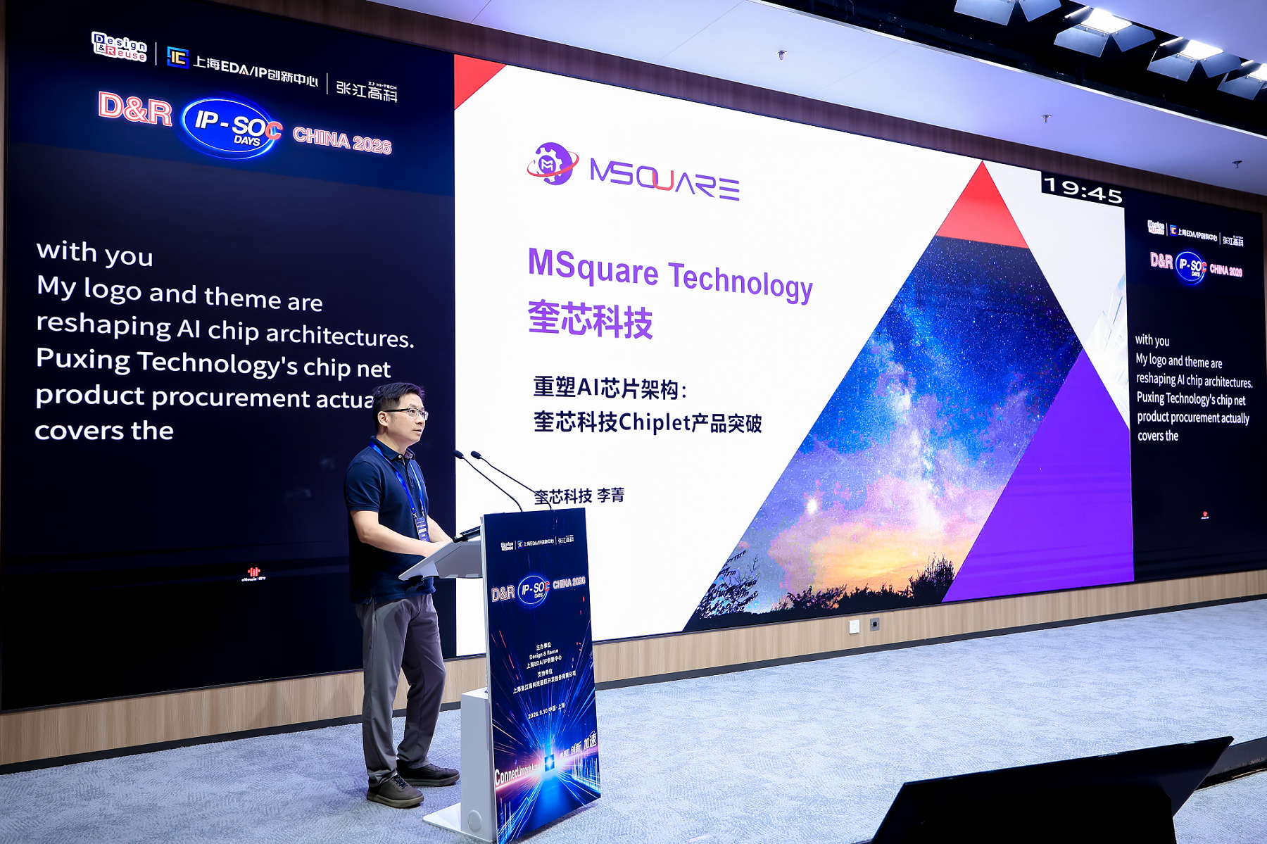
AI:从算力竞争转向互联竞争

报告开篇提出,大模型的发展已经从「算力竞争」进入「互联竞争」。内存带宽与容量需求激增之后,传统IO难以满足Chiplet时代的互联需求,瓶颈从单颗芯片的算力,转移到了系统的数据供给能力。

由此产生的互联需求分为两个方向,二者解决的不是同一个问题:Scale-up关注提升单节点的性能与集成度,依赖D2D(UCIe)与C2C等封装内与芯片间互联;Scale-out关注增加节点数量实现弹性扩展,依赖高速SerDes、可插拔光模块与CXL。低延迟与低功耗直接决定AI应用的可用性与成本效益——这也是D2D互联近两年从「可选项」变成「架构前提」的重要原因。

奎芯科技D2D与Chiplet产品进展

李菁首先分享了奎芯UCIe接口IP的硅上实测数据。 奎芯UCIe方案目前提供Controller与 PHY的完整国产化交付,支持国产标准基板封装,覆盖2D/2.5D封装形态与2 至25mm的互连距离。报告分享了两代测试芯片的实测结果:16 Gbps在 25mm距离下连续测试7 天误码率为0;32 Gbps在同等距离下眼宽23.4ps(0.748 UI),连续72小时误码率为0,并通过25℃ → -40℃ →85℃ →25℃ 的温度循环。功耗低于1.0 pJ/bit,链路训练由硬件完成,D2D link建立时间在毫秒级。

此外,奎芯也实现了同一套IP同时支持D2D与 C2C,客户无需为Die间与芯片间互联各准备一套IP。该能力已在某企业级SSD主控的容量扩展方案中落地——企业级主控SoC通过UCIe连接消费级SoC,实现NAND通道的灵活配置,方案已完成客户流片并量产出货,两种模式均经生产验证。

在接口IP能力完善后,奎芯科技不断加强Chiplet业务产品化、商业化进展。基于UCIe的 IO Die把HBM从主SoC解耦,单颗IO Die带宽匹配一颗HBM3(819GB/s)——先进节点的面积与产能因此节省出来留给计算逻辑;定制化3D Memory则以定制Base Die+ 3D堆叠存储 +UCIe出口的形态,在标准HBM之外提供另一条供给路径——当HBM的供给、价格或用量成为项目的主要约束时,这条路给出的是替换的可能性。

论坛之外,奎芯科技在本届IP-SoC China的展区设立展台,展示了UCIe、LPDDR等IP测试芯片实物以及IO Die方案板,吸引了大量与会者驻足交流。

从论坛到展台,奎芯科技在本届D&R主办的IP-SoC China上传递的是同一个判断:AI芯片的下一程,瓶颈不在单颗芯片的算力,而在系统的数据供给能力。报告结尾,奎芯也强调将继续投入三大方向——IP侧继续深耕高速互联,Chiplet侧打造可复用、可扩展的模块化产品,系统侧打造开放可定制的平台能力。正如报告最后一页所写:AI时代的互联革命,正在由我们共同推动。

注:文/龚作仁,文章来源:Laborer,本文为作者独立观点,不代表亿邦动力立场。

【版权提示】亿邦动力倡导尊重与保护知识产权。未经许可,任何人不得复制、转载、或以其他方式使用本网站的内容。如发现本站文章存在版权问题,烦请提供版权疑问、身份证明、版权证明、联系方式等发邮件至run@ebrun.com,我们将及时沟通与处理。

已点赞

+1

{{ praise_text }}

好文章,值得被更多人看到

FAQ回顾

奎芯科技的UCIe接口IP有哪些核心技术特点?

奎芯UCIe接口IP可提供Controller与PHY的完整国产化交付,支持国产标准基板封装,覆盖2D/2.5D封装形态与2至25mm互连距离;实测传输功耗低于1.0pJ/bit,不同速率下长距离传输误码率为0,可同时支持D2D与C2C互联,链路建立达毫秒级。

当前AI芯片行业的发展瓶颈出现了什么变化?

大模型发展已从“算力竞争”进入“互联竞争”阶段,传统IO难以满足Chiplet时代的互联需求,AI芯片核心瓶颈已从单颗芯片的算力,转移到系统的数据供给能力,互联性能直接决定AI应用的可用性与成本效益。

奎芯科技的Chiplet相关业务有哪些落地进展?

奎芯科技的UCIe互联IP已在某企业级SSD主控容量扩展方案中落地,完成客户流片并量产出货;同时推出可解耦HBM的IO Die、定制化3D Memory方案,可节省先进节点计算产能,提供HBM之外的存储供给路径。

Chiplet时代的互联需求主要分为哪几个方向?

Chiplet时代的互联需求分为两大方向:一是Scale-up方向,聚焦提升单节点性能与集成度,依赖D2D(UCIe)、C2C等封装内与芯片间互联;二是Scale-out方向,聚焦节点数量弹性扩展,依赖高速SerDes、可插拔光模块与CXL技术。

广告

下一篇

跨境电商资源对接

《全球跨境电商服务商资源手册》第二期手册现已发布,触达更多资源,了解跨境服务商信息,欢迎点击链接下载。

了解详情

重磅:亿邦智库 × Pattern栢藤联合发布《智赢·共生—品牌全球化加速增长洞察报告》

当AI重塑消费者的发现与决策路径,平台规则与合规要求日趋复杂,不同区域市场的增长节奏与竞争形态也在加速分化。